Underfill takes on a bigger role as semiconductor packaging shrinks
What is underfill and why is it becoming important?
- How underfill improves the reliability of fine-pitch ball grid array (BGA) connections on printed circuit boards (PCBs)
- Why shrinking electronic packages and higher interconnect density are increasing the need for advanced PCBA reliability processes
- How Ryder Industries uses in-house underfill and fine-pitch SMT manufacturing to support BGA pitches down to 0.2 mm
Research published in Materials Today Electronics shows that higher interconnect density is pushing solder-joint dimensions into the sub-100 μm range in advanced chiplet-based packages, increasing the reliability challenges faced by manufacturers. With AI, automotive, medical and consumer applications driving demand for compact assemblies, techniques traditionally associated with semiconductor manufacturing are now relevant to electronics assembly. Tony Sui, VP of Manufacturing at Ryder Industries, a premium provider of electronics manufacturing services, explains why one of those techniques is underfill.
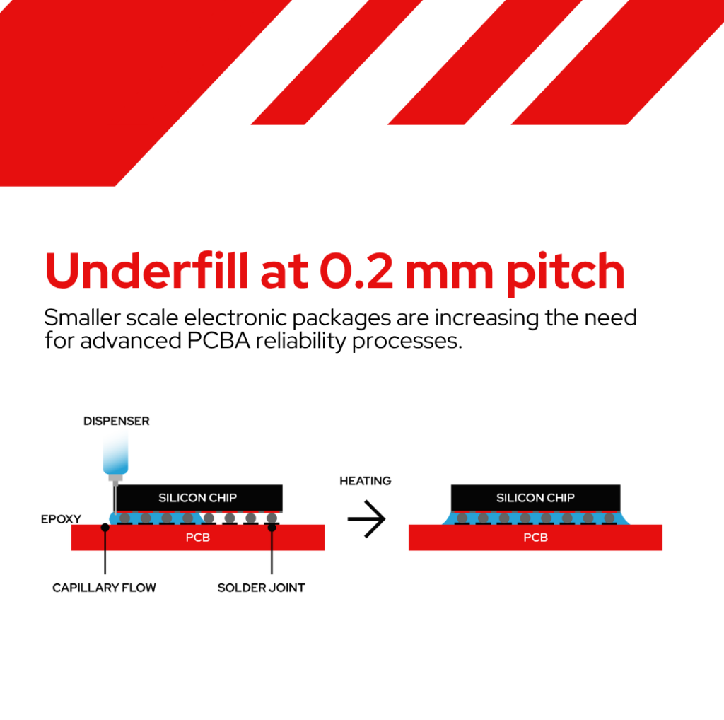
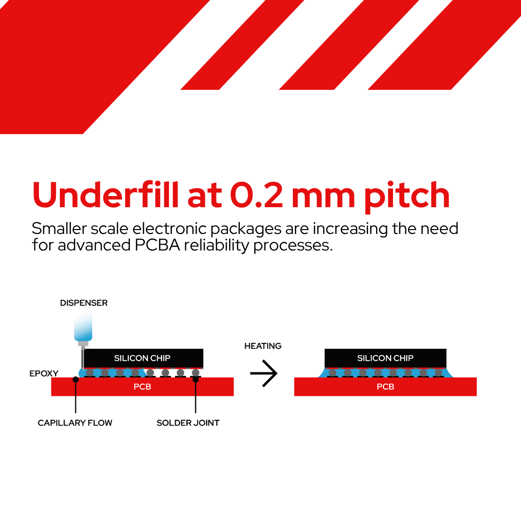
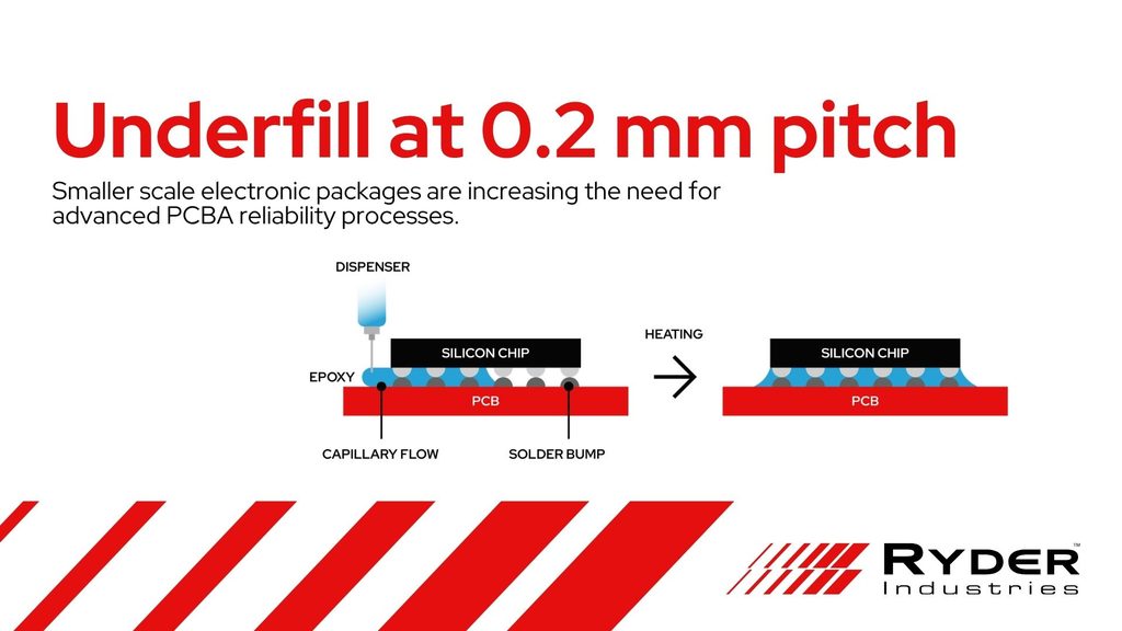
Underfill is typically an epoxy-based material applied beneath components such as ball grid arrays (BGAs). A BGA has an array of tiny gold-plated hemispherical connectors on the underside of the component, which provide the electrical connections to the printed circuit board (PCB).
As designs became smaller and more closely spaced over time, these connections became vulnerable to mechanical and thermal stress. Underfill fills the space beneath the component, holding it firmly in place, evening out thermomechanical stress, mitigating thermal cycling and vibration fatigue, and thereby extending service life in harsh environments.
A main problem which underfill addresses is the difference in coefficient of thermal expansion (CTE) between materials within an electronic assembly. Silicon, metal and PCB substrates expand and contract at different rates as temperatures change, putting stress on solder joints during repeated heating and cooling.
A 2025 review published in Polymers identifies thermomechanical stress as one of the “most pervasive reliability challenges in electronic packaging”. Underfill helps to redistribute this stress away from individual solder joints and across the wider component structure, while also resisting mechanical stresses such as vibration, shock and drop and significantly enhancing board-level reliability.
The principle “Never use an electrical connection as a mechanical support” is widely violated for pragmatic ‘good enough’ reasons. Underfill provides that mechanical support structure and restores design integrity.
From semiconductor manufacturing to EMS
Underfill has long been used in semiconductor and IC manufacturing, but today’s electronic assemblies are incorporating smaller, more sophisticated packages — BGAs, chip-scale packages (CSPs) and system-in-package (SiP) assemblies — that pack more functionality into less space and place greater demands on assembly processes and reliability.
This is most visible in compact modules across automotive, robotics, medical, industrial and AI-related applications, sectors where underfill has traditionally been a semiconductor-manufacturing technique rather than a general EMS one.
Underfill remains a premium capability rather than a routine one: most EMS providers support BGA pitches only down to 0.35 mm, not 0.20 mm.
Reliability and nitrogen reflow
Ryder Industries has developed its underfill process to handle pitches down to 0.2 mm, with pads positioned extremely close together. The smaller the pitch, the less room for manufacturing variation.
The thermal and mechanical stresses on these connections remain unchanged regardless of pitch. Underfill must be part of a wider reliability process involving materials selection, surface preparation, dispensing, curing and inspection.
The underfill material needs to flow consistently through spaces that can be only tens of microns high, before being cured. Ryder’s inspection methods — automated x-ray inspection (AXI), ultrasonic scanning and cross-section analysis — check the finished result.
Thermal cycling can then assess how an assembly performs under repeated temperature changes. JEDEC’s JESD22-A104 standard includes test conditions ranging from -40°C to +85°C, and Ryder has validated its process through 800 cycles over this temperature range.
Reliability and Nitrogen Atmosphere Reflow Soldering
Nitrogen reflow is another SMT capability needed for reliable fine-pitch assembly. The regular reflow process within a normal atmosphere (i.e. with oxygen) has its limitations: oxygen is chemically active, and this leads to spidering (“dendritic growth”) that builds bridges between pads, shorting them out.
Ryder pumps nitrogen gas into the reflow oven to drive out the oxygen, stopping the oxidation of solder and component surfaces. This yields cleaner solder joints, and also lowers the solder’s surface tension so it flows more freely and covers more of the joint, requires less flux and lower peak temperatures and supresses a variety of defect modes: solder voids, graping and tombstoning of ICs, improving yield.
Ryder installed this equipment in 2026. Texas Instruments’ concurs, its: assembly guidance reports shorter wetting times and fewer, smaller voids when using nitrogen compared with air in fine-pitch package assembly.
Ryder’s underfill capability: The proof points
Unlike conventional EMS providers, Ryder applies underfill in-house, integrated into the SMT production flow used for BGA mounting, RF shielding, automated testing and packaging. This eliminates handoff risk, shortens lead times and ensures full process traceability under one roof.
Together, these processes reflect a wider shift across electronics manufacturing. As AI and other high-performance applications demand more functionality from smaller, more highly integrated modules, EMS providers are increasingly being asked to deliver capabilities such as underfill that were once the preserve of semiconductor production.
Unlike conventional EMS providers, Ryder performs underfill in-house, integrated directly into the same SMT production flow used for BGA mounting, nitrogen reflow, RF shielding, automated testing and automated packaging.
The process can accommodate bump pitches down to 0.2 mm, with ball-to-ball spacing approaching semiconductor-grade standards. Testing has also shown near-zero voiding, compared with a typical 4 per cent acceptance target.
Such combination of underfill application, materials, inspection and testing within the same production flow reflects the requirements placed on EMS providers as electronic assemblies become smaller and more densely packed.
Looking for fine-pitch electronics manufacturing support? Find out more about Ryder’s electronics manufacturing services.
FAQs
- When should underfill be used on a PCB?
Underfill should be considered when a PCB assembly contains components that are particularly vulnerable to solder-joint stress, such as fine-pitch BGAs. It can be especially valuable where products face repeated thermal cycling, vibration, mechanical shock or demanding operating conditions, helping improve the long-term reliability of the assembled PCB.
- What is the difference between BGA and underfill?
A BGA (ball grid array) is a type of electronic component package that connects to a PCB through an array of solder balls. Underfill is a separate epoxy material applied beneath the BGA after assembly. It reinforces the connection between the component and PCB, helping protect the solder joints from mechanical and thermal stresses.
- Can underfill improve the reliability of a PCBA?
Yes. Underfill can improve PCBA reliability by helping distribute mechanical and thermal stresses across the solder joints beneath components such as BGAs. This can reduce the effects of thermal expansion differences between the component, solder and PCB, improving resistance to thermal cycling, vibration and mechanical shock.